
Applied Materials (hereinafter referred to as Applied Materials) recently released a new semiconductor manufacturing system that can improve the performance of advanced logic and memory chips required for AI computing. The new products focus on three key areas for developing more powerful AI chips, namely forward-looking logic processes such as GAA, high-performance DRAM such as HBM, and advanced packaging technologies used to create highly integrated system-level packaging and optimize chip performance, power consumption and cost.
Applied Materials pointed out that hybrid bonding is an emerging chip stacking technology that uses direct copper-to-copper bonding to significantly improve overall performance, power consumption and cost. However, due to the increasing complexity of chip packaging, hybrid bonding technology faces challenges in large-scale mass production. In this regard, Applied Materials cooperated with Besi Semiconductor (Besi) to develop the industry's first integrated die-to-wafer (die-to-wafer) hybrid bonding product Kinex™ Bonding bonding system. This system combines Applied Materials' expertise in wafer and wafer front-end processes with Besi Semiconductor's leading die placement, interconnection and assembly with highly precise and high-speed bonding solutions. At present, many leading logic, memory and outsourcing packaging and testing companies (OSAT) have adopted the Kinex system.
Zheng Xinpu, Vice President of Applied Semiconductor Product Business Group and Heterogeneous Integrated Product Technology, said that in the hybrid bonding process, the surface preparation (Surface Preparation) and adhesion (Tacking) steps are the most difficult, and the Kinex system integrates all key hybrid bonding process steps into a single system, which has many major advantages compared to non-integrated solutions.
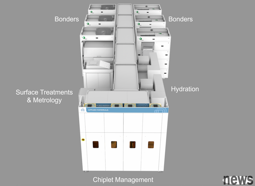
For example, the Kinex system has excellent die-level tracking capabilities to better manage complex multi-die packages; it achieves smaller interconnect spacing through high-accuracy bonding and a clean and controlled environment; it improves bonding consistency and quality by accurately controlling the waiting time between hybrid bonding process steps; and its integrated real-time measurement technology enables faster overlay measurement and drift detection.
Prabu Raja, President of Applied Materials' Semiconductor Product Group, pointed out that as the complexity of chips continues to increase, Applied Materials is focused on promoting material engineering breakthroughs, improving performance and power consumption to meet the needs of large-scale development of AI, and launching earlier and more in-depth cooperation with customers to jointly develop solutions that can accelerate the technology blueprint of chip manufacturers and realize major component changes in the fields of logic, memory and advanced packaging.
In addition to the Kinex system, Applied Materials also launched the new Centura™
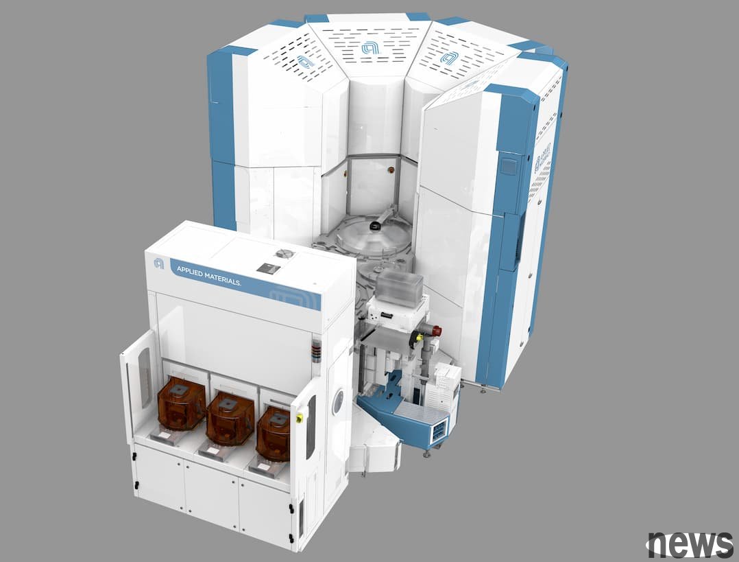
Applied Materials pointed out that the most advanced GAA transistor today has a key characteristic that affects its performance and reliability, which is the source and drain structures. These structures together form the channel of the transistor. The source and drain are formed by precisely depositing materials in deep trenches through an epitaxial (epi) process. In 3D–GAA transistors, filling high aspect ratio source/drain trenches using traditional epitaxial technology is quite challenging and can lead to voids and uneven growth, thereby reducing performance and reliability.
The Xtera system adopts a unique small-volume reaction chamber configuration and integrates pre-cleaning and etching processes to achieve a gap-free GAA source–drain structure, and the gas consumption is reduced by 50% compared to traditional epitaxy. The system's innovative deposition and etching process continuously adjusts the size of the trench opening as the material grows on the sidewalls and bottom of the trench, optimizing the epitaxial growth of billions of transistors on the wafer, achieving no gaps and improving unit-to-unit uniformity by more than 40%. The device has already been adopted by leading logic and memory chip manufacturers.
Another new product, PROVision 10, is a cutting-edge electron beam (eBeam) measurement system designed for advanced logic chips including wrap-around gate transistors and back-side power supply architectures, next-generation DRAM and 3D NAND chips. It is the industry's first measurement system to adopt cold field emission (CFE) technology. Compared with traditional thermal field emission (TFE) technology, it can improve nanometer-level imaging resolution by 50% and increase imaging speed by up to 10 times. The PROVision 10 system's sub-nanometer imaging capabilities enable it to penetrate multiple layers of a 3D chip to provide integrated multi-layer imaging.
Applied Materials pointed out that the system can perform direct on-wafer alignment measurement and accurate critical dimension (CD) measurement, exceeding the limits of traditional optical systems. Its unique capabilities support critical process control tasks such as extreme ultraviolet (EUV) layer alignment and nanosheet pattern measurement, as well as epitaxial void detection in GAA transistors, making it an important inspection tool for advanced processes at 2nm and below, as well as HBM integration. This system is currently used by many leading logic and memory chip manufacturers.
Keith., Vice President of Applied Materials Imaging and Process Control Business Group. Keith Wells (Keith Wells) said that the increasing use of 3D architecture in logic and memory chips brings new challenges to measurement technology and pushes optical technology to its limits. With breakthroughs in imaging resolution, Applied Materials continues its leadership in electron beam technology and conducts in-depth 3D architecture measurements with high productivity, allowing chip manufacturers to obtain accurate measurement data and accelerate the yield of highly complex chip designs.
Further reading: Considering Intel Foundry? Su Zifeng has a conservative attitude and emphasizes in-depth cooperation with TSMC AI chip boom squeezes supply chain! Smartphone SoC key materials may be in short supply for a long time