The world's largest semiconductor device, Dragon Head ASML, has begun to develop the next generation of advanced Weiying equipment to prepare for the chip industry in the next decade. Jos Benschop, the company's vice president of technical executive, pointed out to Japanese that this technology is sufficiently advanced and can meet process requirements after 2035.
Jos Benschop said ASML and exclusive optics partner Carl Zeiss is working on machine designs that can print resolutions to 5-nanometer circuits in a single exposure, and supplementing this technology will be sufficient to meet industry needs in 2035 and beyond.
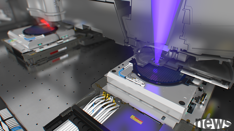
ASML has only recently begun to ship to the first equipment in the industry and has achieved a single exposure of 8 nanometer resolution. In contrast, older equipment must be exposed multiple times to achieve similar resolution, not only has lower efficiency, but also has a certain quality of manufacture.
Benschop pointed out that "we are conducting design research with Zeiss, with the goal of implementing systems with a numerical pore (NA) of 0.7 or above, and no specific timetable has been set yet."
Numerical pores (NA) are key indicators for measuring the ability of optical systems to collect and focus light, and are also key factors in determining whether the circuit diagram can be carefully projected onto the crystal. When the NA is larger and the light wavelength is shorter, the higher the printing resolution is.
The current standard EUV equipment has NA of 0.33, and the latest generation of High NA EUV will be increased to 0.55. While ASML is moving towards NA 0.7 or "Hyper NA" and several key systems need to be redesigned.
ASML has delivered the first batch of High NA EUV equipment to Intel and Taiwan. However, Benschop said that large-scale adoption still takes time. The industry must first verify the performance of the new system and develop supporting materials and tools before it can be fully started. "The introduction of this new equipment is similar to the innovative tools launched in the past year. It usually takes several years to enter the large-scale production stage. Customers need to learn how to operate, but I believe it will be used in high-capacity chip manufacturing processes soon."
ASML commits to developing even more advanced chipmaking tools Extended reading: ASML: Hyper-NA EUV is a major change in the next decade of semiconductors, but the key is cost